What are Microprocessor Architectures?
A Microprocessor Architecture is a definition of the way in which the internal components
of a processor are organised and interact to execute functions and instructions. They can
be classified by instruction sets, complexity, design philosophy, performance aims, power,
speed balance, etc.
Arithmetic Logic Unit, Central Unit and registers are key factors for math & logic
operations, instruction flow management and temporary data storage respectively. They
are connected to memory and I/O devices by data, control and address.
The architectures are broadly split into the CISC and RISC architectures.
The Performance Equation
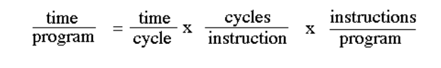
The given image shows the equation used for expressing a computer’s performance.
The CISC architectural approach minimizes the instructions per program even though it
may lead to more cycles per instruction
Meanwhile, the RISC architectural approach reduces the cycles per instruction, sacrificing
the number of instructions per program.
CISC Architecture
What is it?
CISC or Complex Instruction Set Computing is an architecture wherein multiple commands
are executed within a single instruction set with a variable size, minimizing the command
count per program and thus reducing the amount of code required.
History
CISC architecture emerged in the 1950s, the early computer era, wherein, memory was
expensive. This architecture allowed minimization of code size and usage of a single
instruction set to execute multiple complex commands, easing programming without
advanced compilers and saving on memory.
IBM, led by Gene Amdahl, pioneered it with the System/360 mainframe from 1964.
In 1978, Intel further advanced CISC for PCs with the 8086 microprocessor.
The modern x86 Intel and AMD Ryzen processors translate CISC instructions to RISC
micro-ops for efficiency.
Uses
It eased programming, especially in Assembly.
Executing multiple, complex commands, combining data structures and array accesses in
one instruction set, saving memory with smaller program sizes. This is possible as the
architecture directly supports high-level programming constructs like loop control,
addressing modes and procedure calls.
It continues to be the standard architecture in Intel x86 and AMD Ryzen desktops, laptops
and servers. The backward compatibility in softwares prevents full switch to RISC
architecture.
Complex instructions are broken down into subroutines known as microcode
Characteristics
● Complex instructions and complex instruction decoding
● Instruction sets have a variable size
● Instructions can take more than a single clock cycle for execution
● It has numerous complex address modes
● Operations get performed in memory so fewer general-purpose registers in the
chips.
● Supports complex ops in one command.
● Single instructions can perform multiple low level instructions
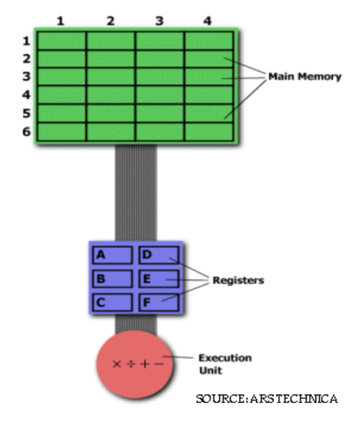
Implementation | The CISC Approach
Taking the image given below for reference. While in standard microprocessor literature chips use hexadecimal linear addresses like 32-bit or 64-bit addresses, let’s say that the main memory contains data from (in row:column format) 1:1 to 6:4. Now, if we want to multiply, for example, the value in 3:1 with the value in 5:4 and input the product in 3:1 to replace the previous value.
To solve this through basic assembly, we would firstly need a hardware processor capable of understanding and executing a series of required operations. Such a processor would likely be prepared with a specific instruction for multiplication, typically MUL. On execution, the instruction would load the integers into two separate registers, multiplies the ops in the execution unit and stores the output in the apt register. This entire task can be completed with a simple instruction MUL 3:1, 5:4 Here, MUL is a complex instruction. Here, it isn’t required to
specifically call a loading or storing function. Alternatively, we can use a higher level
language wherein, we can take 3:1 as a and 5:4 as b and use * for multiplication. In this
way, the command identical to the instruction would be- a = a*b In both cases, the
instruction is short and hence easier to translate to binary
Advantages
● A single instruction can perform multiple low-level operations
● The multiple address modes enhance flexibility
● The code for instructions is shorter, easing programming.
● Since the instructions are smaller, the compiler has less to translate and very less RAM is required for storage.
Disadvantages
● The microprocessors require more power due to variable instruction set sizes
● They require more transistors, increasing cost and heat
● Complex decoding leads to slowed execution and multiple clock cycles.
● CISC processors need to be bigger and hence may not be suitable for smaller devices
RISC Architecture
What is it?
RISC or Reduced Instruction Set Computer is a microprocessor design focusing on small,
optimized instruction sets that would be executed in a single clock cycle.
History
The RISC architecture concept emerged in the 1960s with Seymour Cray’s CDC 6600
implementing load-store architecture. However formal development of the RISC
architecture began in 1975 led by IBM’s John Cocke in the 801 project, eventually
prototyping the first RISC architecture for faster telecom switching in 1980.
Through the 1980s, RISC advanced commercially.
In the 1990s, it expanded with PowerPC and dominated the embedded systems.
A major setback for IBM’s RISC architecture chips was Intel with their CISC processors even
though they were losing popularity, Intel possessed resources for thorough development
and production of powerful processors
Now, in 2026, RISC-V is open source and gains traction in IoT and AI.
Examples
● ARM, a.k.a the Advanced RISC Machine- It is globally the most widely used RISC
architecture. It powers IoT devices, smartphones, tablets, the Apple M-series
Macbooks, etc.
● RISC-V- It is an open source instruction set architecture that enables companies to
design custom chips without needing to pay licensing fees. It’s gaining significant
traction in IoT, AI acceleration and embedded systems.
● IBM Power a.k.a PowerPC- It has a historical significance in Apple Macintosh
computers and iconic gaming consoles like Xbox 360, Wii, Playstation 3. Even now,
it is essential in various IBM supercomputers and servers.
● Atmel AVR- It’s a prominent 8-bit architecture found in microcontrollers like
Arduino
● MIPS- It’s one of the earliest commercial architectures. It previously powered
Nintendo 64 and Playstation 1. While it’s not as prominent in current PCs, it can
still be found in industrial controllers and networking equipment like routers.
● SPARC- It was developed by Oracle and used in Unix workstations and
high-performance servers
● DEC Alpha- It was used in supercomputers and high-end workstations in 1990s,
famous for its extreme performance until it was discontinued due to high
manufacturing costs, corporate acquisitions, etc.
● Microchip PIC- It’s widely used in automotive systems and embedded controllers.
Uses
The modern x86 Intel and AMD Ryzen processors translate CISC instructions to RISC
micro-ops for efficiency
RISC-V allows companies to modify chips without any licensing fees, becoming a major
focal point.
They use multiple, longer but simpler instructions which include separate instructions for
load and store to execute a command in a single clock cycle.
It powers nearly all modern smartphones and tablets using ARM architecture. It’s
responsible for handling apps, graphics and AI processing efficiently.
It’s ideal for microcontrollers where low power and customization are required.
Characteristics
It has constant length, simple instructions.
It uses load/store only operations to move data to/from memory from registers where the
operation occurs.
It has many registers to minimize memory access
It uses pipelining to divide instructions into distinct stages to overlap the execution of
multiple commands so that the instruction is completed in a single clock cycle. Pipelining
helps in a uniform, fixed instruction size and simplicity.
They are smaller
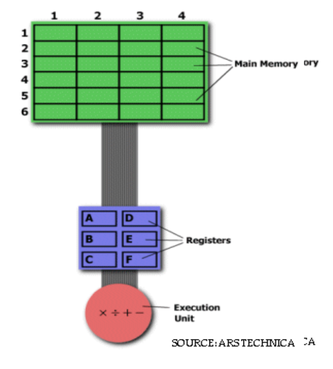
Implementation | The RISC Approach
Taking the image given below for reference. While in standard microprocessor literature chips use hexadecimal linear addresses like 32-bit or 64-bit addresses, let’s say that
the main memory contains data from (in row:column format) 1:1 to 6:4. Now, if we want to multiply, for example, the value in 3:1 with the value in 5:4 and input the product in
3:1 to replace the previous value. To solve this using basic assembly, we will have to first load
the values individually onto the register using the LOAD function. We would give the values a variable to define them. Once the values are loaded, we can proceed to multiply them using the MUL function. By default, the output would replace the first value in the register which we need then to store it back in the memory and we would do this using the STORE function. Hence, we would require 3 commands to get our desired request
LOAD A, 3:1
LOAD B, 5:4
MUL A, B
STORE 3:1, A
While there are more lines of code, this makes the instruction simpler for the RAM and
compiler.
Advantages
● Simpler hardware helps in easier pipelining and hence a faster execution time
● Higher clock speeds. Instructions are executed in a single clock cycle.
● It requires lower power as the instructions are simpler, there are lesser transistors
and a simpler design
● It enables chips to be smaller, battery optimized and results in less heating
● It helps in better compiler optimization and scalability
Disadvantages
● The programs are longer and hence require more memory for storage
● To perform a complex operation, you require multiple small, simple, typically
one-worded instructions and so the capabilities of the architecture are limited
● RISC microprocessors are often more expensive
-Saanvi Verma